AI CapEx Cycle Series, industry primer. Written so that even a reader new to semiconductor front-end (Front-End) processing can follow it — from the economics of the clean room, through the step-by-step oligopoly, the one-to-two-year lag from CapEx to equipment revenue, and Korea's materials-parts-equipment coverage — this rebuilds the industry's skeleton from the ground up. Part 1 is the front end; Part 2 (the back end) follows
Semiconductor front-end investing is a game of total CapEx, not of individual-company share wars. With a winner fixed at each step — ASML 100% of EUV lithography, Tokyo Electron 90% of coater/developers, KLA 56% of metrology — once the memory big three and foundries fix their capital spending, the allocation across equipment makers is decided almost mechanically. So a forecast of total CapEx becomes a forecast of equipment-maker revenue, and the typical one-to-two-year lag from a CapEx announcement to equipment revenue recognition is the key variable deciding the trade timing of Korea's front-end materials-parts-equipment names.
Reader's Brief — 30-second TL;DR
Intro
Why Now
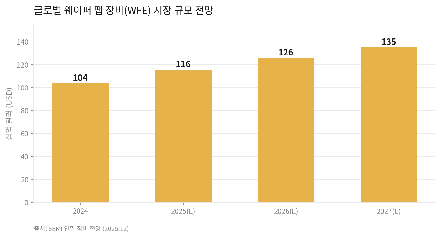
Of the roughly $133 billion in global semiconductor equipment sold in 2025, wafer fab equipment (WFE) was $115.7 billion — more than six times the back-end equipment market — and SEMI projects $135.2 billion by 2027. Korea's 2026 equipment spending will rise 27% year over year to about $29.7 billion, projected to return to the world's number-two spot. In June, domestic front-end equipment names surged (SOL Semiconductor Front-End ETF +38.1%, PSK +64.3%, Wonik IPS +48.1%, HPSP +40.4%), pre-reflecting the expectation. The next readings are the memory big three's quarterly CapEx guidance and domestic equipment makers' supply-contract disclosures.
Winners ?? Losers
The beneficiary structure: demand for AI-training HBM and inference/storage NAND lifts the memory big three's CapEx, which is transmitted to the step-by-step oligopoly makers (ASML, Tokyo Electron, Lam Research, KLA) and to their one-year-lagging derivative layer, Korea's materials-parts-equipment (deposition: Wonik IPS, Jusung Engineering, Eugene Technology, Tes; cleaning: PSK; high-pressure hydrogen annealing: HPSP; photoresist: Dongjin Semichem). The pressure: June's rally pre-reflected the expectation, leaving room for correction in high-valuation names amid an earnings vacuum (Jusung Engineering PBR 14.2x), and if a hyperscaler CapEx slowdown transmits into a pace adjustment by the memory big three, the derivative layer is pressured first. The monitoring priority is the two clocks — the direction of total CapEx and individual order disclosures.
Watch For
Reading depth
§ 01 The Industry's Center of Gravity — Why Start With the Front End
Making a single semiconductor chip splits broadly into two stages. The front end etches invisible circuits onto a silicon wafer; the back end cuts, stacks, connects, and tests the finished wafer into a final product. In a cooking analogy, the front end is the kitchen where ingredients are prepped into a finished dish, and the back end is the hall where the dish is plated, packaged, and inspected.
Follow the money and the center of gravity is clear. On SEMI's year-end forecast, global semiconductor sales in 2025 were about $133 billion, of which wafer fab equipment (WFE) — the front-end portion — was $115.7 billion. That is more than six times the back-end equipment market of $11.2 billion in test equipment plus the low-$6 billion range in assembly and packaging equipment. To invest in semiconductor equipment is, in most cases, to invest in front-end equipment.
Figure 1. Global wafer fab equipment (WFE) market size forecast (SEMI, December 2025)
The engine of growth is AI. AI training needs high-bandwidth memory (HBM), and inference and data storage need NAND; this demand is lifting the capital spending of the memory big three (Samsung Electronics, SK Hynix, Micron). According to SEMI, Korea's 2026 equipment spending will rise 27% year over year to about $29.7 billion, returning to the world's number-two spot behind China. High-bandwidth memory expansion sits at the center of it.
So the conclusion — the front-end equipment market is where AI infrastructure capital is ultimately paid, and its size is on a path to set a fresh record every year through 2027. Without understanding the front end, you see only half of a materials-parts-equipment investment.
§ 02 From Sand to Chip — the Front End at a Glance
2.1 The Wafer — the Purest Disc in the World
Everything starts with the wafer. A wafer is a thin, 300mm-diameter (about 30cm) disc made by refining silicon drawn from sand to an extreme purity. On this pizza-sized disc, hundreds of fingernail-sized chips are made at once. Because electricity will not flow as designed if purity drops even slightly, the wafer is at once the most basic and the most demanding material in semiconductors.
2.2 A Circuit Is Not "Drawn" but "Stacked and Sculpted Layer by Layer"
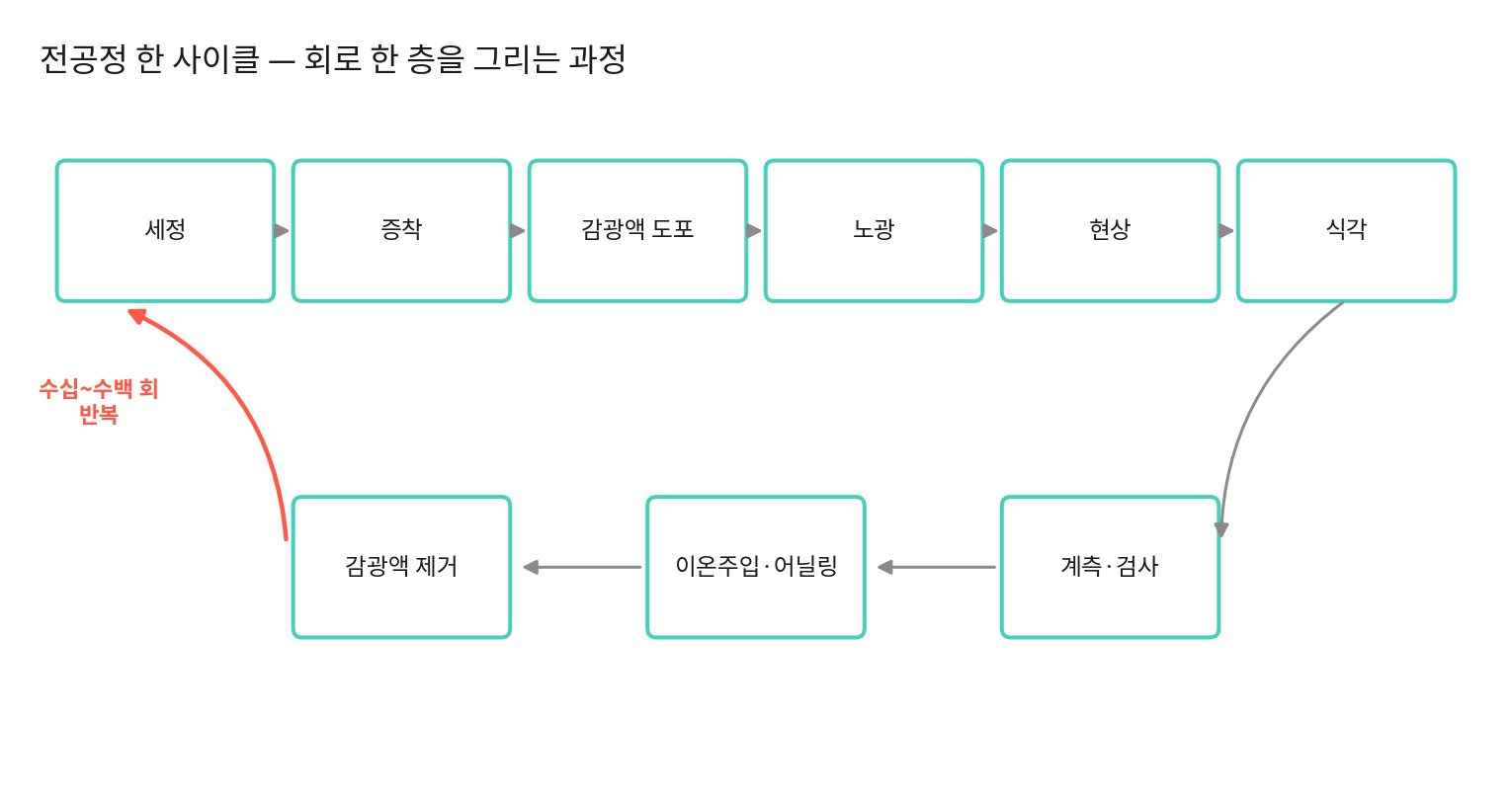
Many people imagine a semiconductor circuit is made like drawing with a pen, but in reality it is closer to constructing a building. You stack one thin film (deposition), print the blueprint onto it with light (lithography), carve away what is unnecessary (etch), and wash it clean (cleaning) — repeating for every single . Once dozens of such layers are stacked, you get a three-dimensional structure of tens of billions of interconnected transistors: the chip. It amounts to erecting a high-rise city on the wafer.
Figure 2. One front-end cycle — the repeating loop that makes a single circuit layer
2.3 The Explosion in Step Count — How Miniaturization Creates Equipment Demand
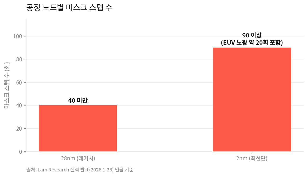
As circuits shrink, the number of layers and process steps grows explosively. According to what Lam Research disclosed on its January 2026 earnings call, a legacy 28-nanometer (nm) process ran fewer than 40 mask steps, whereas a leading-edge 2nm wafer goes through more than 90 mask steps and about 20 extreme-ultraviolet (EUV) exposures. More steps means more equipment is needed to make the same volume of wafers.
Figure 3. Mask-step count by process node
This is the structural reason the front-end equipment market grows faster than semiconductor revenue itself. Even if chip demand does not rise, equipment demand rises simply because the process gets finer. Layer on top of that the volume expansion AI has triggered, and you have the current cycle.
So the conclusion — the front end is a process that repeats a "stack, print, sculpt, wash" loop hundreds of times, and as miniaturization advances, the count of that loop itself rises, structurally growing equipment demand.
§ 03 The Economics of the Clean Room — Dissecting a $20 Billion Fab
Key Points
—Why this is investment information.
3.1 A Single Speck of Dust Can Topple a City
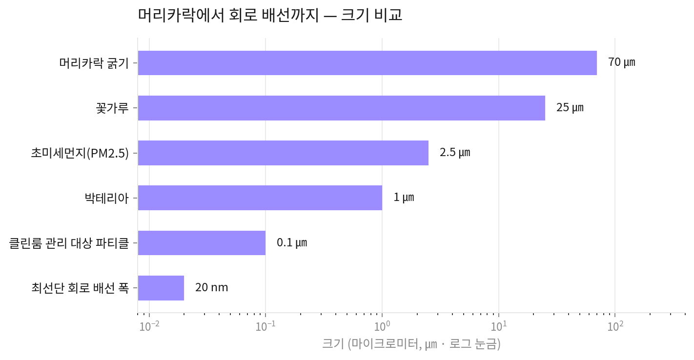
The factory where the front end takes place is called a fab. The heart of a fab is the clean . Why must it be this clean? A leading-edge chip's wiring width is a few tens of nanometers (nm) — a few thousandths of the thickness of a human hair. If a single 0.1-micrometer (µm) particle floating in the air lands on a circuit, that chip fails, as if a boulder had dropped onto a road.
Figure 4. From a human hair to a circuit wire — a size-scale comparison (log scale)
So a clean room's class is defined by the particle count in the air. The international standard (ISO 14644-1) grades cleanliness from class 1 to class 9 by the number of particles in a cubic meter of air, and a semiconductor fab's core zones are managed at the strictest end, ISO class 3-5. For reference, the ordinary indoor air we live in does not even reach the lowest class on this scale. Because people themselves are the biggest source of contamination, workers wear cleanroom suits and move only along set paths.
3.2 The Fab's Vertical Structure — the Clean Room Is the Middle of a Four-Layer Sandwich
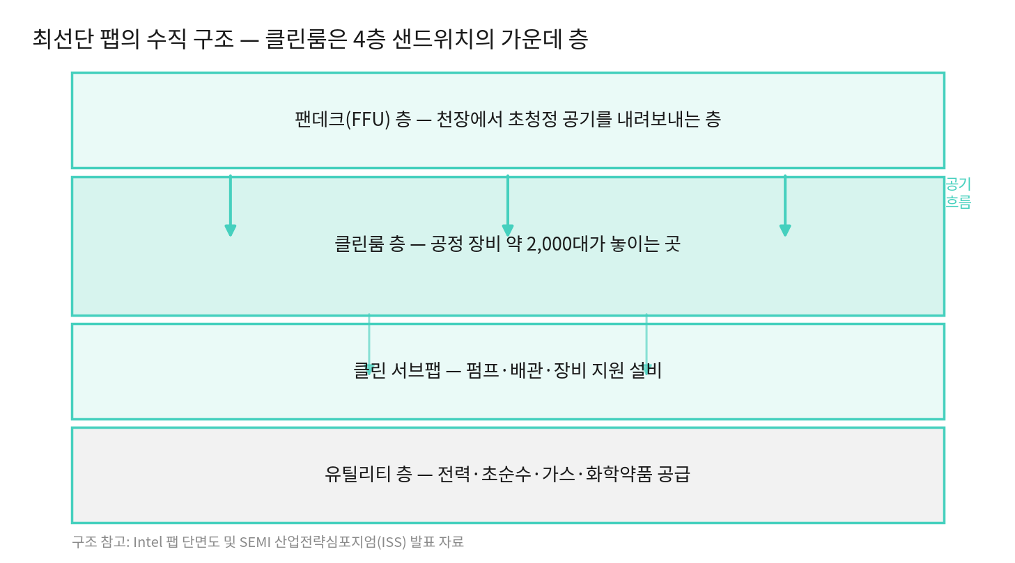
A clean room is not simply a clean space but an entire building that is one giant air-purification machine. Fan filter units (FFUs) installed on the top fan deck push ultra-clean air downward; the air passes vertically through the clean room, exits through perforated floor panels into the layer below, then recirculates through the filters again. It is designed so that any particle generated is immediately washed downward.
Figure 5. The vertical four-layer structure of a leading-edge fab and its air flow
The sub-fab below the clean room houses vacuum pumps, piping, and gas and chemical supply equipment, and from the lowest utility layer come power, ultra-pure water (water stripped of impurities to the extreme), and specialty gases. A leading-edge fab consumes millions of gallons of ultra-pure water a day, making it one of the most resource-intensive facilities on Earth.
3.3 Where Does the $20 Billion Go
According to a presentation at SEMI's Industry Strategy Symposium (ISS), the total investment in a single leading-edge fab exceeds $20 billion, of which the building structure itself is $4-6 billion. It is a mega civil-engineering project consuming 83,000 tons of steel, 785,000 cubic yards of concrete, and 30-40 million man-hours of work — yet even so, about three-quarters of the total is not the building but the price of the roughly 2,000 process tools that go inside it.
Clean-room construction itself is a different order from ordinary building. Construction cost for a high-purity semiconductor clean room is estimated at $2,500-7,500 per square foot, of which the air-handling and filtration system accounts for 35-55% of the project cost. The floor must be flat to within 0.5mm over a 3-meter span, and vibration is controlled for the sake of the lithography tools. A fab is less a building than one giant precision machine in itself.
Why this is investment information. A fab construction announcement is a preview of equipment orders. Because the physical timetable from groundbreaking to clean-room completion to tool move-in is set, fab news can be read as a leading indicator of equipment-maker revenue one to two years out. The link is the fact that most of the is not the building but the equipment.
So the conclusion — the clean room is the result of turning an entire building into a machine to wage war on particles, and the essence of a $20 billion fab is not the concrete but the 2,000 tools inside it. That is why fab groundbreaking news matters to materials-parts-equipment investors.
Full access requires 🥉 Bronze tier
Sign in with Google — your tier will be checked automatically and access granted if eligible.
This site runs on ads — the tier system rewards community contributions.
Comments
This report is provided for informational purposes only and does not constitute a recommendation to buy or sell any financial instrument. Investment decisions should be made based on your own judgment and responsibility. The analysis and opinions contained herein are based on information available at the time of writing and are subject to change.